




A Ten-Thousand-Word Analysis of the “Optical Interconnect” Industry Chain: The AI Infrastructure Bottleneck Overshadowed by GPU Brilliance
TechFlow Selected TechFlow Selected
A Ten-Thousand-Word Analysis of the “Optical Interconnect” Industry Chain: The AI Infrastructure Bottleneck Overshadowed by GPU Brilliance
The explosive growth of GPU computing power is pushing optical interconnects to become a new bottleneck in AI infrastructure. CPO technology is reshaping the industrial chain landscape, unlocking billion-dollar market opportunities across the entire value chain—from upstream substrates to downstream foundry services.
 Navigating Web3 tides with focused insights
Compiled & Translated by TechFlow
Host: Nico
Original Title: AI Optical Interconnects: The Next Trillion-Dollar Market Hidden in the Glow of GPUs?
Podcast Source: Nico Frontier Alpha
Air Date: May 8, 2026
Editor’s Introduction
Optical interconnects are evolving from “supporting components” for GPUs into the core bottleneck of AI data centers. When hundreds or even thousands of GPUs must collaborate within a single rack, across racks, or across super-nodes, actual computational efficiency is determined not only by chips themselves—but by the data transmission capacity between GPUs.
This episode adopts an industry-investment research perspective to map out the entire optical interconnect value chain—from optical modules and silicon photonics PICs (photonic integrated circuits), to CPO (co-packaged optics), external lasers, InP substrates, SOI substrates, foundry services, and packaging & testing—providing a tiered investment framework spanning AVGO, MRVL, GLW, COHR, LITE, TSEM, SIVE, AAOI, AXTI, IQE, and Soitec.
The most important takeaway from this episode is not a stock recommendation, but a strategic judgment: AI infrastructure competition is shifting from “who has more GPUs” to “who can secure access to the scarcer optical interconnect supply chain.” CPO may represent the largest incremental variable in this transition.
Key Quotes
Why Optical Interconnects Suddenly Matter
- “Even if an NVIDIA GB300 GPU accelerator card delivers immense compute power, most of that power goes to waste if it cannot communicate at high speed with thousands of other GPUs.”
- “Insufficient interconnect bandwidth makes purchasing additional GPUs a highly inefficient investment.”
- “Whether for training or inference, any collaborative workload requires high-speed data exchange between GPUs—the data pathway enabling this is the interconnect.”
- “Optical interconnects are not hype—they address a real, urgent, and irreversible demand in AI data centers.”
Copper Cables Exit Stage Left; Fiber Optics Take Center Stage
- “Copper cable transmission speeds have nearly hit their physical limits—bandwidth per copper wire has reached its ceiling.”
- “Signal attenuation and interference begin after just a few meters of copper cabling, yet AI data center interconnections routinely span tens or even hundreds of meters.”
- “Fiber optic bandwidth is dozens of times greater than copper, supports distances up to several kilometers, and consumes negligible power.”
The Industrial Essence of Optical Modules
- “Optical modules handle communication between racks—not between GPUs inside a single rack.”
- “The optical module supply chain and the GPU supply chain are not independent markets; GPU shipment volumes directly drive optical module demand.”
- “Manufacturing an optical module spans two entirely distinct semiconductor process ecosystems: InP compound semiconductors for optical chips, and silicon for DSP chips.”
The Real Significance of CPO
- “CPO does not disrupt a single component inside optical modules—it redefines the optical module product form itself.”
- “CPO is not an upgrade or replacement of existing products, but a fundamental architectural reconstruction.”
- “More precisely, CPO opens an entirely new market—one far larger than the pluggable optical module market—not merely substituting for the existing one.”
Investment Framework Across the Value Chain
- “Unlike the GPU market dominated by NVIDIA, the optical interconnect supply chain features extremely fine-grained specialization and highly dispersed bottlenecks.”
- “The further upstream you go, the smaller the companies—and the higher their growth potential—but the lower their predictability. Conversely, downstream companies are larger, more predictable, but offer less upside.”
- “If you can tolerate high risk and volatility, the core logic is to target bottlenecks—each bottleneck is typically served by only one or two companies.”
Beyond GPUs: The Truly Scarce ‘Nervous System’ of AI Infrastructure
For the past two to three years, almost everyone has been discussing GPUs and computing power. Since the launch of ChatGPT—the generative AI product from OpenAI that ignited the large language model (LLM) application wave—and the subsequent explosion of the AI technology revolution, NVIDIA’s stock price has surged fifteenfold over three years. Computing power has become an indispensable keyword for AI LLMs, and the GPU-centric semiconductor supply chain has entered a golden era transcending economic cycles.
Yet over the past year, another critical—and arguably even scarcer—element has quietly exploded: In large-scale data center deployments, even the most powerful NVIDIA GB300 GPU accelerator card becomes largely ineffective if it cannot communicate at high speed with thousands of other GPUs. Insufficient interconnect bandwidth renders massive GPU purchases inefficient. This element responsible for enabling high-speed communication among thousands of GPUs is optical interconnects.
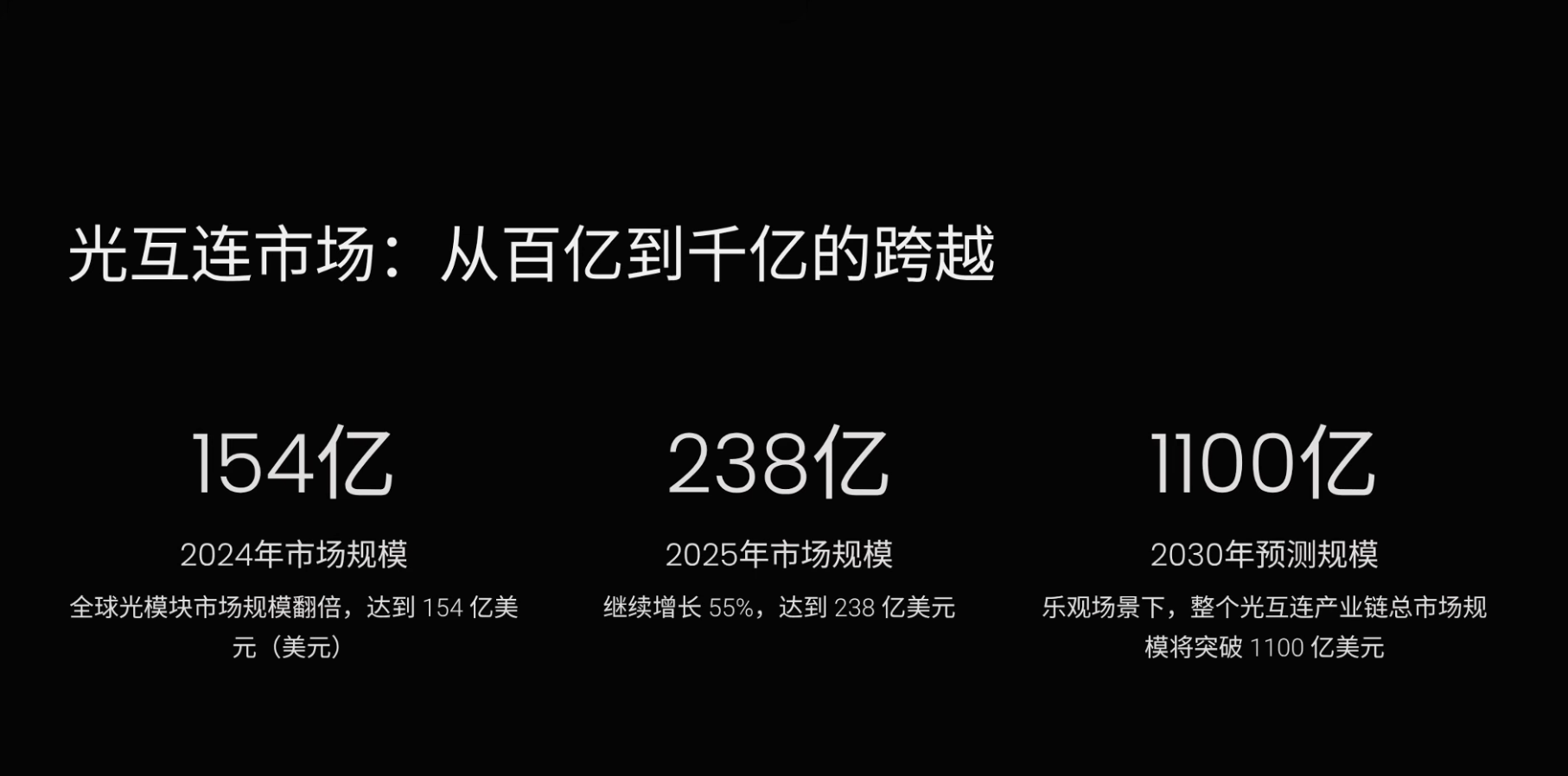
According to LightCounting—a research firm specializing in optical communications—the global optical module market doubled in 2024 to $15.4 billion; it grew another 55% in 2025 to $23.8 billion. Under an optimistic scenario, LightCounting forecasts the total optical interconnect supply chain market will exceed $110 billion by 2030.
Yet most investors likely haven’t heard of many companies on this supply chain. SIVE/SIVEE, with annual revenue of ~$30 million, has surged tenfold since the start of 2026; TSEM (Tower Semiconductor)—an Israeli specialty foundry dubbed “the TSMC of optical interconnects”—has already booked 70% of its capacity through 2028; COHR (Coherent), a vertically integrated company in optics and materials, generates ~$5.8 billion in annual revenue and has received a $2 billion strategic investment from NVIDIA.
Today’s episode dissects the optical interconnect supply chain from end to end: What are optical interconnects? What’s inside an optical module? What is the next-generation technology roadmap? Where are the key bottlenecks? Which companies sit where along the chain? And how should investors allocate across this sector based on their individual risk preferences?
Training, Inference, and Interconnects: Why High-Speed GPU Communication Is Essential
Before diving into specific companies, let’s first answer why optical interconnects have suddenly become one of the most critical and scarce elements in AI infrastructure. To understand this, we need to start with how AI works—through two phases: training and inference.
Training involves feeding massive amounts of text, images, and code into a model, allowing it to continuously learn and evolve from existing data. Training parameters for large models can reach trillions—far exceeding the memory capacity of any single GPU. Therefore, the model must be partitioned across thousands of GPUs for parallel computation. After each GPU completes its assigned portion, intermediate results must be transmitted to other GPUs to collaboratively complete the full task.
Inference is when AI applies learned knowledge to generate responses—for example, asking ChatGPT a question and receiving an answer within seconds. Many assume inference only requires one GPU answering one query—no interconnect needed. That may have held true in 2023, but it’s completely different by 2026.
AI has evolved from simple Q&A to deep reasoning and agentic AI. Users no longer interact with basic chatbots but with complex agents capable of task planning, multi-step reasoning, and querying multiple data sources. Behind each interaction may lie coordinated work by hundreds—or even thousands—of GPUs. Whether for training or inference, any collaborative workload demands high-speed data exchange between GPUs—the data pathway enabling this is the interconnect.
Why Copper Cables Are No Longer Enough
Historically, interconnects relied on copper cables transmitting electrical signals. Now, fiber optics carrying optical signals are gradually replacing them. Copper cables fall short for three main reasons.
First, copper transmission speeds have nearly reached their physical limits. No matter how much materials or fabrication processes improve, bandwidth per copper wire has plateaued—like a two-lane highway where only two cars can pass side-by-side, regardless of traffic density. Second, signal quality degrades with distance. Copper cables begin attenuating and suffering interference beyond just a few meters, while AI data center connections routinely span tens or hundreds of meters—far beyond copper’s capability. Third, copper cables consume significantly more power. GPU power consumption rises with each generation—H100 draws 700W, B200 jumps to 1kW, and GB300 will be even higher. At these power levels, copper interconnects between GPUs themselves consume substantial electricity.
Fiber optics are fundamentally different. A single fiber offers bandwidth dozens of times greater than copper, transmits reliably over several kilometers, and consumes negligible power. Fibers also support simultaneous transmission of multiple wavelengths—like a highway divided into eight lanes, each carrying light of a different color without interference. One fiber effectively replaces dozens of copper cables.
The Three Phases of Optical Interconnects in Data Centers
Optical interconnects in data centers did not appear overnight—they evolved through clearly defined stages. With each stage, optical connectivity moves progressively closer toward the chip.
Phase One occurred before 2020. Back then, optics were used mainly between data centers—for example, connecting cloud providers’ facilities in Beijing and Shanghai, separated by over 1,000 km via fiber. Within data centers, however, servers still communicated primarily via copper cables.
Phase Two spanned 2023–2024. ChatGPT’s late-2022 launch ignited the AI technology revolution, triggering explosive GPU sales the following year. Yet the optical module market did not initially respond. At the time, NVIDIA GPU clusters still relied heavily on copper cables; optical modules were not considered core components. Compounding matters, cloud providers cut capital expenditures amid recession fears early in 2023—Meta (Facebook’s parent company and one of the world’s largest cloud and AI infrastructure buyers) slashed its optical module deployment plan by over half.
The real turning point came in 2024. Cloud providers scaled GPU clusters from hundreds to thousands—even tens of thousands—of units, rendering copper’s meter-level transmission range wholly inadequate. NVIDIA replaced copper with pluggable optical modules in its reference architecture—a structural shift that ignited the market, doubling optical module revenues in 2024.
Phase Three began in 2025 and continues today. NVIDIA’s Blackwell architecture—the latest AI GPU platform—is deployed at scale, demanding even higher power and interconnect bandwidth—driving further surges in optical module demand. Meanwhile, the top five cloud providers collectively spent over $300 billion on capital expenditures in the first nine months—setting a new record—and optical module demand briefly exceeded supply by more than double, creating severe imbalance. In March this year, NVIDIA invested $2 billion each in Lumentum and Coherent. At GTC 2026 (NVIDIA’s annual developer conference), NVIDIA showcased its CPO solution and next-generation Rubin architecture optical interconnect design—effectively declaring optical interconnects a central narrative in AI infrastructure, not a niche subplot.
What Is an Optical Module? The Translator Between Electrical and Optical Signals
Before delving into investment analysis, let’s clarify some foundational concepts. First: optical modules. GPUs natively process electrical signals, while fibers carry optical signals—two incompatible languages requiring a translator that converts electrical signals to optical ones for transmission, and vice versa upon reception. That translator is the pluggable optical module.
An optical module is roughly the size of a USB drive—plugged into a server’s network interface card (NIC) on one end and connected to fiber on the other. Large AI data centers may contain tens or even hundreds of thousands of these “small boxes.” A common misconception: optical modules handle communication between racks—not between GPUs inside a single rack.
Take NVIDIA’s GB300 NVL72—an entire rack-level GPU system—as an example. Each rack houses 72 GPUs interconnected via NVIDIA’s NVLink and NVSwitch technologies—all using copper-based electrical signaling over distances of mere centimeters to one or two meters, requiring no optics. Only when data must travel from one rack to another—distances of tens or hundreds of meters—do optical modules come into play.
In a full AI cluster, optical modules are typically installed in two places: on server NICs and on switches. Each fiber requires an optical module at both ends. More GPUs, more racks, and more inter-rack connections mean greater optical module demand. Thus, the optical module supply chain and GPU supply chain are not independent—they’re tightly coupled, with GPU shipments directly driving optical module demand.
The Five Core Components of an Optical Module
A USB-drive-sized optical module contains five core components: laser diode chip, modulator chip, photodetector chip, DSP (digital signal processor) chip, and lens/fiber coupling assembly.
First is the laser diode chip. Its function is to emit stable laser light as the optical signal carrier. Think of it as a miniature flashlight—smaller than a fingernail—yet emitting precise, pure light. The most critical aspect is material. GPUs and CPO use silicon, whereas lasers rely on indium phosphide (InP) or gallium arsenide (GaAs). Silicon is inherently poor at light emission; compound semiconductors like InP and GaAs possess atomic structures better suited for photon generation—explaining why laser chips aren’t fabricated by silicon foundries like TSMC.
Second is the modulator chip. The laser emits raw, information-free light—a “blank beam.” The modulator encodes electrical signals onto this light. Binary electrical signals (0s and 1s) from the GPU are converted into corresponding light intensity variations—turning the laser on/off or modulating brightness to represent digital data. Continuing the analogy: the laser is a constantly lit flashlight; the modulator is the hand flicking its switch billions of times per second. Sometimes, the modulator and laser reside on the same chip—called an EML (electro-absorption modulated laser)—integrating flashlight and switch into one component.
Third is the photodetector chip. While the modulator converts electrical signals to optical ones (transmission), the receiver must convert optical signals back to electrical ones—requiring a photodetector. It acts like the ear at the receiving end: detecting light outputs “1,” absence of light outputs “0.” Photodetectors also commonly use InP or GaAs material systems.
Fourth is the DSP chip (digital signal processor). It serves as the optical module’s “brain,” performing error correction, encoding, and signal equalization. Optical signals degrade during transmission—like trying to hear someone clearly on a noisy highway. The DSP encodes signals at the transmitter and cleans noise at the receiver to ensure reconstructed 0s and 1s match original data. As a silicon-based chip, the DSP shares the same semiconductor process ecosystem as GPUs and CPO—typically manufactured by silicon foundries like TSMC.
800G and 1.6T refer to optical module data rates: 800 gigabits per second and 1.6 terabits per second—doubling speed. Optical modules progressed from 400G to today’s mainstream 800G and now emerging 1.6T. Higher speeds increase chip design complexity—and raise DSP cost and design difficulty, sometimes exceeding that of the laser itself.
Fifth is the lens and fiber coupling assembly. Its job is to precisely align the laser’s narrow beam with the tiny fiber core—just one-tenth the diameter of a human hair—requiring micron-level alignment accuracy. Imagine threading a needle through another needle’s eye—repeated millions of times automatically on a factory production line.
Stringing these five components together reveals the optical module’s workflow: GPU electrical signals first enter the DSP for encoding and error correction, then proceed to the modulator; the modulator encodes the electrical signal onto the laser’s optical beam; light passes through the lens into the fiber, traveling tens to hundreds of meters; at the far end, light exits the fiber, is aligned by the lens onto the photodetector; the photodetector converts light back to electrical signals, passed to the receiving DSP for decoding and error correction, finally delivered to another GPU.
How Optical Modules Are Made: Two Parallel Semiconductor Process Flows
Many assume all chips are made by TSMC—so optical module chips should be similar. Reality is entirely different. An optical module contains two fundamentally distinct chip types—built on two different materials and manufactured in two separate foundry ecosystems.
First are DSP chips—the “brains” of optical modules, handling error correction and encoding. These are silicon-based chips, sharing similar manufacturing processes with GPUs and CPO, produced by silicon foundries like TSMC. Key DSP design firms include AVGO (Broadcom—communications and custom AI chip giant), MRVL (Marvell Technology—data center and networking chip company), and CRDO (Credo—data interconnect chip company).
Second are optical chips—including lasers, modulators, and photodetectors—fabricated using compound semiconductors like InP. Some companies handle both design and manufacturing in-house—e.g., LITE (Lumentum—optical communications devices and lasers), COHR (Coherent—optical materials and devices), and AAOI (Applied Optoelectronics—U.S.-based optical module and device company). Others specialize in laser design—e.g., SIVE/SIVEE—pushing laser performance to extremes before outsourcing fabrication to foundries.
Optical chips cannot be manufactured by TSMC because its entire production line—equipment, chemicals, and process parameters—is optimized exclusively for silicon. InP is a completely different material: wafer sizes, etching chemicals, and growth temperatures differ substantially—rendering TSMC’s lines unusable for InP. Thus, optical chips have their own independent manufacturing ecosystem.
Substrates and Epitaxy: The Two Foundations of Optical Chip Manufacturing
To understand optical chip manufacturing, two concepts are essential: substrates and epitaxy. Substrates are the starting point for all optical chips—a specialized thin wafer upon which functional layers grow. Think of planting a light-emitting “laser tree”: seeds won’t take root in ordinary sand but require special soil whose molecular structure matches the seed. Ordinary silicon is like sand—unsuitable for light emission; InP is that special soil.
Substrate quality directly determines the quality of all subsequent layers. An atomic-scale defect in the substrate propagates upward like a crack, causing laser chips to fail specifications and optical modules to be scrapped. Producing ultra-pure InP substrates is extremely difficult—only a handful of global manufacturers can do so consistently.
Having a substrate isn’t enough—you must grow functional layers atop it, a process called epitaxial growth. Lasers emit light not because the substrate itself glows, but because specially engineered structures grown on it emit photons when electrons and holes recombine under current flow.
Each epitaxial layer is only nanometers thick—stacked like a multi-layer cake. Composition, thickness, and doping concentration must meet extreme precision requirements: missing even one atomic layer shifts emitted wavelength, rendering the laser unusable.
InP substrates are supplied by AXTI (U.S. compound semiconductor substrate supplier); epitaxy is performed by IQE/IQEE (U.K. compound semiconductor epitaxy supplier). After epitaxy, laser chip manufacturing follows two paths: fabless (design-manufacturing separation)—e.g., Swedish SIVE/SIVEE designs lasers, then outsources fabrication to Taiwan’s Win Semi (Vanguard International Semiconductor Corporation, a compound semiconductor foundry); or IDM (integrated device manufacturing)—e.g., LITE, COHR, and AAOI handle everything from epitaxy and lasers to modulators, photodetectors, and final optical module assembly.
Thus, optical module manufacturing spans two entirely distinct semiconductor process ecosystems: InP compound semiconductors for optical chips, and silicon for DSP chips. These are incompatible—cannot share production lines. Any bottleneck anywhere halts the entire optical module supply chain.
This explains why optical companies rarely venture into DSP design—and digital chip firms avoid lasers. Optical chip design and digital chip design are entirely different disciplines. Optical engineers master laser physics, optical waveguide theory, and quantum well structures; digital chip engineers focus on logic circuits and digital signal processing algorithms. Skills don’t overlap—like cardiac surgeons and neurosurgeons: both are surgeons, but can’t swap operating rooms.
This is what makes the optical interconnect supply chain fascinating. Unlike the GPU market dominated by NVIDIA, it’s characterized by extremely fine-grained specialization and highly dispersed bottlenecks. Precisely because of this dispersion, ordinary investors can uncover small, overlooked companies.
CPO: Moving Optical Components from Server Backplanes to Chip-Side
Pluggable optical modules are today’s standard—but a fundamental restructuring is underway. A next-generation technology called CPO (co-packaged optics) is poised to completely reinvent the optical interconnect architecture.
CPO stands for co-packaged optics. It solves the problem of optical modules being too far from GPUs. Today’s standard places optical modules as pluggable boxes on server backplanes—GPU electrical signals must traverse tens of centimeters of copper traces to the backplane before conversion to optical signals. These centimeter-scale copper runs cause energy loss, latency, and heat. As AI cluster density increases, these tiny losses amplify millions of times into serious issues.
CPO’s approach is to move optical components from server backplanes into the chip package itself—positioning them adjacent to GPUs or switching chips—reducing electro-optical conversion distance from centimeters to millimeters. Analogy: today’s setup separates rice and soup—GPUs are in the rice bowl, optical modules in a separate cup; CPO pours the soup into a dedicated compartment within the rice bowl—rice and soup remain separate, but now reside in the same container, just millimeters apart.
But integrating optical components into chip packages faces a major obstacle: traditional optical chips use InP, while GPUs use silicon—InP and silicon packaging processes are incompatible. You can’t simply integrate InP chips and silicon-based GPUs into the same package. The solution is to build optical chips from silicon—introducing silicon photonics PICs.
PIC stands for photonic integrated circuit. Familiar ICs integrate billions of transistors onto a single chip for computation; PICs follow the same concept—but integrate optical components instead of transistors. A silicon photonics PIC integrates modulators, optical waveguides, photodetectors, and other functions onto a single silicon chip. Being silicon-based, it can leverage packaging technologies similar to those used for GPUs—an impossibility for InP optical chips.
Silicon photonics PICs don’t use ordinary silicon wafers—they use SOI (silicon-on-insulator), a special sandwich-structured wafer. An insulating layer between substrate and top silicon confines light propagation to the thin top silicon layer, preventing leakage downward. Ordinary silicon wafers are solid blocks—light scatters uncontrollably; SOI’s insulating layer acts like a mirror, reflecting light back into the top layer to guide it along designed channels.
SOI substrates are supplied by French firm Soitec—one of the dominant players in this niche, approaching monopoly status. Silicon photonics PIC foundry services are led by TSEM (Tower Semiconductor). TSEM fabricates silicon photonics chips on SOI wafers using modified CMOS processes—technologies unfamiliar to TSMC, making TSEM the highest-share foundry in this specialized domain.
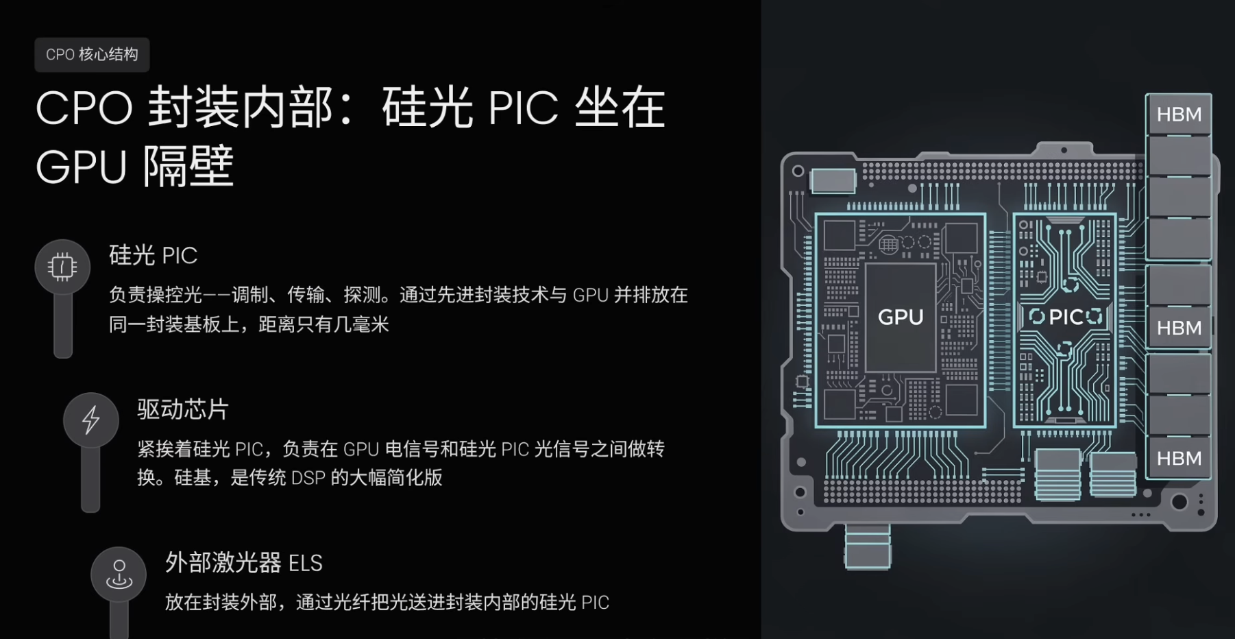
However, silicon has a fundamental limitation: it doesn’t emit light. Thus, silicon photonics PICs can manipulate light—but not generate it—requiring external InP lasers as light sources. This forms CPO’s core architecture: a silicon photonics PIC inside the package handles modulation, transmission, and detection; it’s placed adjacent to the GPU or switch chip on the same package substrate—just millimeters away, akin to HBM memory sitting beside the GPU.
Beside the silicon photonics PIC resides a driver chip—converting GPU electrical signals to silicon photonics PIC optical signals. Also silicon-based, it’s essentially a simplified version of the traditional optical module’s DSP. Because CPO’s electro-optical conversion distance is only millimeters, complex DSP error-correction and encoding become unnecessary—simple drivers suffice.
Outside the package sits the external laser source (ELS), delivering light into the silicon photonics PIC via fiber. Lasers aren’t placed inside the package because InP lasers generate significant heat—packing them alongside GPUs and silicon photonics PICs would cause thermal issues; plus, lasers have finite lifespans—if integrated into the package, failure would scrap the entire multi-thousand-dollar chip. Making lasers external and pluggable allows direct replacement without affecting the chip itself.
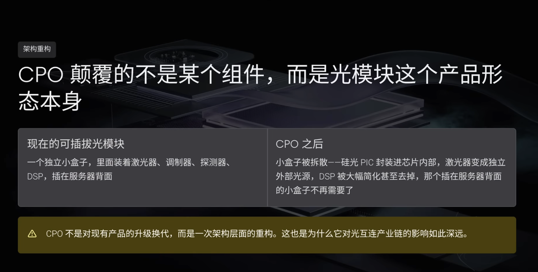
What CPO truly disrupts isn’t a single optical module component—but the optical module product form itself. Today’s pluggable optical module is a standalone box housing lasers, modulators, photodetectors, and DSPs. CPO dismantles this box: silicon photonics PICs embed directly into chip packages; lasers become standalone external light sources; DSPs are drastically simplified or eliminated; the small box on the server backplane disappears. This isn’t an upgrade—it’s a foundational architectural reconstruction.
Why CPO Became an Investment Theme in 2026
CPO has existed for years—why did it suddenly become a hot investment theme in 2026? Goldman Sachs published a report projecting the optical interconnect market’s potential to expand from ~$15 billion today to $154 billion by 2028—a ~9x increase—with CPO accounting for $91 billion. The sole core reason: NVIDIA’s next-generation architecture has shifted CPO from optional to mandatory.
In the current GB300 NVL72 system, 72 GPUs form a single rack—interconnected internally via copper cables. But as AI clusters scale to hundreds or thousands of GPUs, inter-rack network connections become the bottleneck. For its next-generation Rubin platform (NVIDIA’s codename for its upcoming AI platform), NVIDIA introduces CPO for inter-rack network switches—replacing traditional pluggable optical modules. This marks NVIDIA’s first official adoption of CPO within its own platform.
By the subsequent Feynman platform (NVIDIA’s codename for its next-next-gen AI platform), CPO may even extend to intra-rack GPU interconnects—meaning optics are progressively moving from inter-rack to intra-GPU proximity. Lumentum’s CEO confirmed on its latest earnings call that CPO will face massive supply-demand imbalance—demand vastly exceeding supply—and identified CPO as Lumentum’s largest single growth driver—still in its very early stages.
Industry data shows CPO’s current shipment volume remains minimal—around $160 million in 2026, mostly samples and small batches. Yet if Goldman Sachs’ forecast materializes, it will explode to $91 billion by 2028—a zero-to-$100-billion hyperbolic curve. NVIDIA began mass-producing CPO switches in early 2026; Broadcom delivered CPO-related products to customers in October 2025; TSMC launched its COUPE (CPO advanced packaging solution). With both NVIDIA and Broadcom adopting CPO, it’s no longer a distant concept—it’s becoming reality.
Nonetheless, CPO won’t replace pluggable optical modules in the near term. CPO targets ultra-dense AI cluster internal connections—e.g., GPU interconnects within NVIDIA’s super-nodes. Data centers still require vast numbers of other connections—rack-to-switch, switch-to-switch, and data-center-to-data-center—which will continue relying on pluggable optical modules for the foreseeable future. Thus, the more accurate relationship is that CPO creates a new market—potentially far larger than the pluggable optical module market—not merely substituting for it. Both will coexist across different use cases.
Five Benefiting Segments If CPO Explodes
If CPO truly explodes—or enters a super-cycle—the five most-benefited segments along the value chain are:
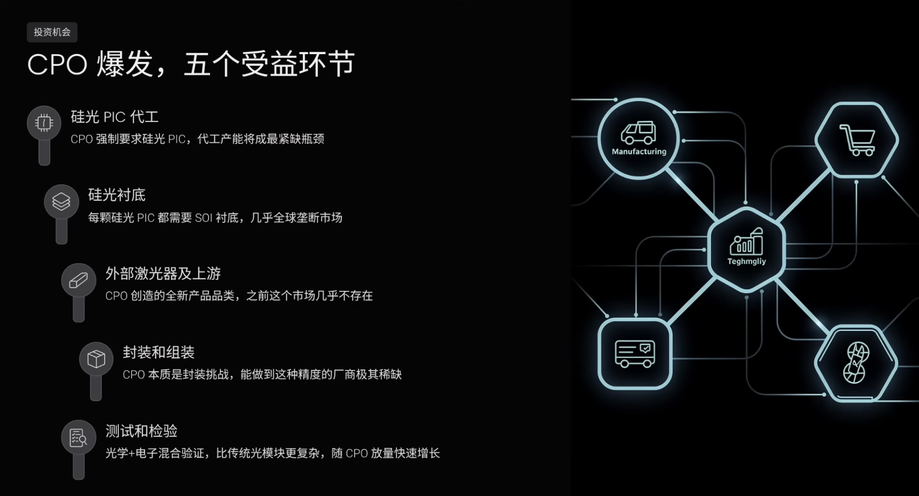
First is silicon photonics PIC foundry services. CPO mandates silicon photonics PICs—only silicon-based chips can be co-packaged with GPUs. Few foundries can produce silicon photonics PICs—capacity will become one of the tightest bottlenecks.
Second is silicon photonics substrates. Every silicon photonics PIC requires an SOI substrate; CPO-driven demand for silicon photonics PICs will massively boost SOI substrate demand—already a near-global monopoly market.
Third is external lasers and their upstream supply chain. CPO creates a new product category: traditional pluggable optical modules integrate lasers inside the box; CPO architectures require lasers to be externalized as standalone light sources. Previously, this market barely existed.
Here lies a critical mismatch in manufacturing capacity. Major laser manufacturers’ existing capacity focuses on EML (electro-absorption modulated laser) lasers—integrating light emission and modulation on a single chip for pluggable optical modules—orders already booked through 2027–2028. But CPO needs simpler lasers—emitting light only, with modulation handled by the silicon photonics PIC inside the package. Though both use InP, these lasers differ in design and production lines—making seamless transitions impossible. Large manufacturers’ capacity is locked into traditional laser contracts—forcing even Lumentum to procure CPO lasers from the open market—creating overflow demand for independent laser suppliers.
Laser demand surge will cascade upstream: more lasers require more InP substrates and more epitaxial wafers. Goldman Sachs warns InP substrate shortages could persist through 2027.
Fourth is packaging and assembly. CPO is fundamentally a packaging challenge—requiring ultra-precise integration of silicon photonics PICs and electronic chips. Firms capable of CPO-grade packaging and assembly will become extremely scarce.
Fifth is testing and inspection. Every silicon photonics PIC requires optical performance testing and reliability validation before shipment. CPO testing is more complex than traditional optical modules—requiring hybrid optical-electronic verification—making this segment grow rapidly alongside CPO volume.
In summary, CPO demand explosion most benefits silicon photonics foundry, silicon photonics substrates, external lasers, InP substrates and epitaxy, packaging/assembly, and testing/inspection—these bottleneck segments.
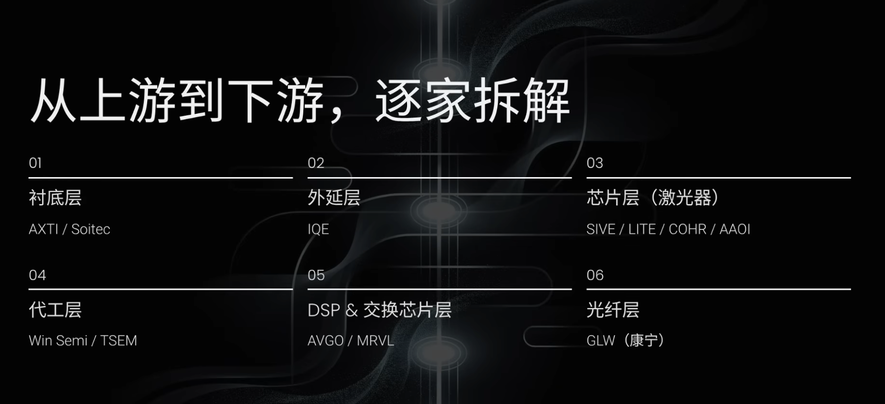
Upstream Substrates: AXTI and Soitec
Moving from upstream to downstream, the two most critical substrate companies are AXTI and Soitec. They serve different technical pathways—not competitors but collaborators. AXTI serves the laser supply chain (light generation); Soitec serves the silicon photonics supply chain (light manipulation). Optical interconnects require both.
AXTI is a U.S. company producing InP and GaAs substrates. Its work involves purifying, synthesizing, and growing single-crystal ingots from rare elements like indium, phosphorus, gallium, and arsenic—then slicing them into wafers. AXTI’s irreplaceability lies in its globally limited pool of high-quality InP substrate producers—besides AXTI, only Japan’s Sumitomo Electric and Germany’s Freiberger hold comparable capabilities. AXTI’s moat includes material purity process expertise, decades of know-how, and lengthy customer qualification cycles. Switching suppliers requires full revalidation of product lines—high switching costs.
CPO won’t bypass InP substrates—it will amplify demand. Under CPO, each GPU requires an external laser—laser count directly ties to GPU count. More lasers mean more InP substrates. Thus, CPO is unambiguously positive for AXTI. Its investment profile: small market cap, high volatility, demand lag, but potentially large stock price elasticity once orders materialize.
Soitec is a Paris-listed French company producing SOI silicon photonics substrates. Soitec dominates the silicon photonics-specific SOI substrate market and invented the Smart Cut patent—its proprietary SOI wafer manufacturing technology. CPO’s core is silicon photonics PICs—each requiring SOI substrates—making Soitec a highly certain beneficiary of the CPO super-cycle. Its valuation stood at ~1.4x book value—low for a global monopolist. Note: Soitec trades on Euronext Paris—not U.S. exchanges.
Epitaxial Layers: IQE/IQEE
Next down the chain is epitaxy. A major independent epitaxial supplier is IQE/IQEE—listed in London. IQE’s moat lies in epitaxy’s extreme difficulty: building functional layers like a multi-layer cake atop substrates—each only nanometers thick—where minute deviations in materials, temperature, or growth time can render lasers unusable. These parameter combinations constitute “epitaxial recipes”—IQE has accumulated decades of such recipes—impossible to replicate quickly with money alone.
With CPO’s explosion, IQE’s logic mirrors AXTI’s: CPO amplifies laser demand—more lasers require more epitaxial wafers. IQE’s risk lies in high customer concentration—LITE is a key client. If LITE pursues vertical integration and brings epitaxy in-house, IQE’s largest revenue stream could be disrupted—a single-point risk investors must consider.
Laser Chips: SIVE/SIVEE, LITE, COHR, AAOI
Proceeding downstream to the chip layer—the most scarce segment is lasers. Core companies include SIVE/SIVEE, LITE, COHR, and AAOI.
SIVE/SIVEE is one of the fastest-rising optical interconnect names over the past year. A Swedish-listed microcap (~$1.5B market cap, ~$30M annual revenue), it follows a semi-fabless model—owning its InP100 platform and a small Glasgow-based wafer fab with some manufacturing capability—while partnering with Taiwan’s Win Semi to scale high-power laser production via mature foundry capacity.
SIVE/SIVEE holds five core advantages. First, its InP100 standardized platform modularizes laser core components—enabling rapid configuration of diverse products like building blocks. Second, wafer-level testing—testing chips directly on wafers instead of cutting and testing individually—boosts yield and cuts costs. Third, coverage of both current and next-gen tech—offering lasers for pluggable optical modules and CPO external light sources. Fourth, multi-track diversification—serving AI data center interconnects, LiDAR, satellite comms, and defense—mitigating single-market risk. Fifth, asset-light expansion—using small fabs for core validation and low-volume production, scaling mass production via Win Semi’s capacity—avoiding heavy CAPEX while retaining core manufacturing control.
SIVE/SIVEE is a high-beta CPO super-cycle play. One reason: large manufacturers’ capacity is locked into traditional laser orders—overflow CPO external light source demand falls to independent suppliers. Another: it’s embedded in multiple CPO project supply chains. AMD’s CPO solution leverages GlobalFoundries’ platform—SIVE is one of few laser suppliers in that ecosystem; Marvell’s Celestial AI (silicon photonics interconnect startup) and Ayar Labs (CPO/silicon photonics startup) are also clients.
Yet SIVE/SIVEE carries clear risks: low revenue, most customers still in development/validation—not yet in mass production. If just two or three customers ramp, the stock could surge; delays or cancellations could trigger sharp pullbacks. View it as a high-odds lottery ticket.
LITE (Lumentum) represents the IDM (integrated device manufacturing) laser path—handling laser design, fabrication, and full optical module assembly. LITE’s key catalyst is NVIDIA’s $2 billion strategic investment and multi-billion-dollar procurement commitment—locking in its capacity. Additionally, LITE is deeply integrated with Google’s TPU (Google’s custom AI accelerator chip ecosystem)—with Google’s AI data centers widely deploying LITE’s optical circuit switching technology and lasers.
LITE’s CEO made three critical statements on its earnings call: CPO will face massive supply-demand imbalance; CPO is LUMENTUM’S LARGEST SINGLE GROWTH DRIVER; CPO REMAINS IN ITS VERY EARLY STAGES. This amounts to frontline industry confirmation of the CPO super-cycle. LITE’s capacity is booked through 2028—its moat: dual anchor customers—NVIDIA and Google. Risk: capacity lock-in with NVIDIA implies short-term growth ceilings—revenue depends heavily on NVIDIA orders—limiting company autonomy and flattening growth curves versus SIVE/SIVEE’s steeper trajectory.
COHR (Coherent) is a rare full-stack optical interconnect company—covering materials, InP lasers, silicon photonics PICs, and optical modules across the entire value chain. Its optical module market share ranks among the global top tier—~20%. Like LITE, COHR secured NVIDIA’s $2 billion strategic investment and multi-billion-dollar procurement commitment.
COHR’s advantage is resilience across technological evolution—whether CPO demands silicon photonics PICs (it makes them), lasers (it makes them), or pluggable optical modules (it makes them). That’s the value of full-stack coverage. COHR resembles a mid-cap, higher-safety optical interconnect play—high certainty, less upside than SIVE/SIVEE, but lower volatility and risk.
AAOI is one of few U.S.-based vertically integrated optical interconnect companies. It uses MBE (molecular beam epitaxy) equipment to grow epitaxial layers on InP substrates—fabricating laser chips, assembling optical subassemblies, and integrating finished optical modules. Its core business is 800G and 1.6T pluggable optical modules. The transcript notes AAOI secured its first major 1.6T data center optical module order in March—exceeding $200 million—and a $71 million 800G order in April.
AAOI won’t necessarily be disrupted by CPO. First, pluggable optical modules won’t vanish with CPO’s rise—CPO addresses super-node internal connections, while vast inter-rack connections still require pluggable modules. Second, AAOI is entering the CPO supply chain. Under CPO, lasers can’t reside inside packages—they must be externalized as small modules delivering light via fiber. AAOI’s newly unveiled product is precisely an external laser source for CPO. Overall, AAOI’s strengths are vertical integration, U.S.-based manufacturing enhancing supply chain security narratives, and laser technology extending into CPO external light sources. Yet it remains a small-cap, high-beta name—volatile, high-upside, high-risk.
Foundries: Win Semi and TSEM
After lasers, consider foundries—the two most critical are Win Semi and TSEM.
Win Semi is one of the world’s largest pure-play compound semiconductor foundries—offering both GaAs and InP foundry services. SIVE/SIVEE’s laser mass production relies heavily on Win Semi. Next-gen CPO architecture amplifies external laser demand—making Win Semi the most critical foundry partner for laser design firms. Regardless of which laser design firm ultimately wins, Win Semi will likely manufacture them.
TSEM is an Israeli specialty foundry dubbed “the TSMC of optical interconnects.” It may be among the most directly benefited companies in the CPO super-cycle. CPO’s core is silicon photonics PICs—and TSEM is the highest-share silicon photonics PIC foundry. CPO’s mandate for silicon photonics PICs elevates TSEM’s silicon photonics foundry business from a niche segment to the center of the value chain.
TSEM’s capacity is largely booked through 2028—yet its forward P/E remains only 16–18x—leaving room for upside amid high CPO growth expectations. Core risk: geopolitical—being an Israeli company located in the Middle East exposes it to regional conflict risks.
Win Semi and TSEM are both foundries—but differ fundamentally in materials and output. Win Semi manufactures lasers using InP and GaAs—responsible for light generation; TSEM produces silicon photonics PICs on SOI substrates—responsible for light manipulation. These material systems are incompatible—they’re not competitors but complementary foundry partners serving different value chain segments.
DSP and Switch Chips: Broadcom and Marvell
Next down the chain are DSP and switch chips—dominated by Broadcom and Marvell.
Broadcom (AVGO) is a trillion-dollar U.S. stock giant—operating across switch chips, custom AI accelerator chips, enterprise software, and more. Its optical interconnect-relevant businesses fall into two areas. First, DSP chips—the “brains” of optical modules handling error correction and encoding—Broadcom is a leading supplier here. Second, CPO switches—Broadcom’s third-generation CPO switches have entered mass production—novel switches integrating optical engines directly beside switch chips. On CPO commercialization timing, Broadcom is even ahead of NVIDIA.
Yet from an investment perspective, optical interconnects represent only one of Broadcom’s many businesses—contributing modestly to overall revenue. Its stock won’t multiply several-fold solely due to CPO’s success. Investing in Broadcom means buying broad AI infrastructure certainty—not single-point CPO explosiveness.
MRVL (Marvell Technology) is another diversified chip company—spanning custom AI accelerators, data center networking chips, and storage chips. Its optical interconnect-relevant businesses also fall into two areas. First, DSP chips—Marvell and Broadcom are the two dominant suppliers in this space, competing head-to-head. Second, CPO—Marvell acquired Celestial AI, significantly strengthening its silicon photonics interconnect capabilities.
This episode’s core thesis is that GPU interconnects are shifting from copper to optics. Celestial AI pursues the same direction—just at shorter distances: replacing copper with optics inside chip packages. Through this acquisition, Marvell’s strategic position in CPO is markedly enhanced.
Compared to Broadcom, Marvell’s optical interconnect exposure is more concentrated. Broadcom is a trillion-dollar entity—optical interconnects are just one piece; Marvell is smaller—$8.2B in last fiscal year’s revenue (+42% YoY)—with management forecasting near $15B over the next two fiscal years. Optical interconnects and CPO contribute a larger share of Marvell’s total revenue—offering greater upside. Marvell isn’t a pure-play optical interconnect stock—but may be the best-balanced choice spanning both DSP and CPO domains.
Underlying Fiber: Corning (GLW)
Finally, the foundational layer: GLW (Corning). Corning is the global leader in optical fiber. Many recognize Corning from Apple iPhone display glass—but optical communications is now one of Corning’s largest and fastest-growing divisions. Since inventing telecom fiber in 1970, Corning has laid millions of miles of fiber cable.
No matter which optical module company wins—or whether the technology path favors pluggable modules or CPO—Corning’s fiber remains indispensable. Under CPO, lasers and silicon photonics PICs still connect via fiber—and inter-rack connections continue using fiber. Fiber is one of the few segments in the entire value chain unaffected by technology-path debates.
Corning recently secured strong customer commitments. In January, Meta announced up to $6 billion to help Corning expand its fiber cable factories; NVIDIA signed a multi-year agreement with Corning—investing $500 million for Corning equity. Corning pledged to increase U.S. optical connectivity capacity tenfold, boost fiber output by over 50%, and build three new factories.
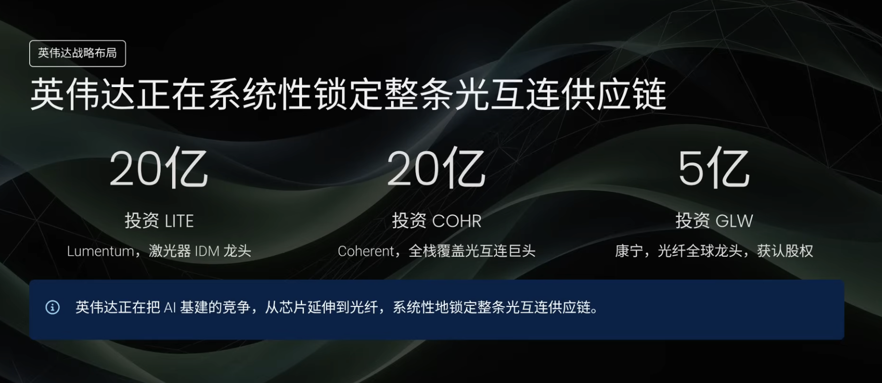
NVIDIA previously invested $2 billion each in LITE and COHR—now adding $500 million to Corning—demonstrating NVIDIA’s systematic effort to extend AI infrastructure competition from chips to fiber—locking in the entire optical interconnect supply chain. Corning represents the highest-certainty, lowest-upside play across the optical interconnect value chain.
Three Portfolio Allocation Strategies: Conservative, Balanced, Aggressive
Having covered numerous companies, the final question is: “How to invest?” The most important pattern is: upstream companies are smaller, offering higher upside—but lower certainty; downstream companies are larger, offering higher certainty—but lower upside. Upstream substrate and epitaxy firms like AXTI and IQE have small market caps and demand lags—but explosive upside once demand ramps. Downstream giants like AVGO offer high certainty—but unlikely to surge 5x in a year.
Strategy One: Conservative Allocation—core holdings are AVGO, MRVL, and GLW. All are relatively large-cap firms—Broadcom’s market cap stands at ~$2 trillion, ranking among the top 10 U.S. stocks; Marvell and Corning hover near the $100 billion mark. Broadcom and Marvell are diversified—optical interconnects represent only part of their businesses; Corning, though more focused, supplies fiber—a technology-path-agnostic necessity. This portfolio offers limited downside—other businesses can support stock prices even if optical interconnects underperform—ideal for long-term investors unwilling to bear high volatility.
Strategy Two: Balanced Allocation—core holdings are COHR, LITE, and TSEM. All are leaders in their respective segments—mid-sized firms balancing certainty and upside. COHR is a full-stack optical company resilient across technological directions—NVIDIA’s $2 billion investment provides a safety net; LITE is NVIDIA’s locked-in laser supplier—its CEO personally confirmed CPO supply-demand imbalance; TSEM is the highest-share silicon photonics PIC foundry—valued relatively cheaply. This portfolio suits investors seeking optical interconnect exposure while tolerating moderate volatility.
Strategy Three: Aggressive Allocation—core holdings are SIVE/SIVEE, AAOI, Soitec, AXTI, and IQE. All occupy upstream bottleneck segments. SIVE/SIVEE is a scarce CPO external laser supplier—embedded in multiple CPO supply chains; AAOI is a high-beta pluggable optical module play—also capable of supplying CPO external lasers; Soitec dominates silicon photonics substrates; AXTI supplies InP substrates for laser manufacturing; IQE produces critical epitaxial wafers for lasers. If the CPO super-cycle unfolds at Goldman Sachs’ projected pace, this portfolio offers maximum upside—but also highest risk.
These small-cap names can easily drop 20–30% in a single day—allocate no more than 5–10% of your total portfolio here. Also note: many optical interconnect small-caps aren’t listed on U.S. exchanges—Soitec trades on Euronext Paris, IQE on the London Stock Exchange, SIVE in Sweden, Win Semi in Taiwan. Interactive Brokers supports most—but requires enabling corresponding market permissions.
Risk Factors: CPO Timeline, NVIDIA’s Choices, Small-Cap Volatility
The entire sector carries notable investment risks.
First, CPO commercialization timing remains uncertain. Goldman Sachs’ $91 billion CPO market forecast is highly aggressive. Achieving this requires NVIDIA’s next-gen architecture launching on schedule, CPO yields meeting targets, InP substrate supply keeping pace, cloud providers sustaining high capex, and continuous capital inflow into the supply chain. Any single link breaking would reduce the final number.
Second, NVIDIA’s choices are pivotal. Which optical interconnect solution NVIDIA selects for its Rubin platform will directly shape the entire supply chain landscape. While NVIDIA has incorporated CPO into Rubin’s reference architecture, specific supplier selection and mass-production timelines remain fluid.
Third, small-cap names carry inherent risks. Many optical interconnect supply chain firms have tiny market caps—never overweight them, and never leverage positions.
Three Core Judgments and Closing Thoughts
Finally, my three core judgments on the optical interconnect sector.
First, optical interconnects are not hype. AI data center interconnect demand is real, urgent, and irreversible. The more GPUs sold, the greater the optical interconnect demand—a certainty tightly coupled to the GPU supply chain.
Second, CPO is the largest future growth vector in this sector. Goldman Sachs projects the optical interconnect market could grow 9x—with CPO accounting for $91 billion; Lumentum’s CEO personally confirmed severe CPO supply-demand imbalance—and its early-stage status; NVIDIA has embedded CPO into its next-gen architecture—confirming it’s not a distant story, but unfolding reality.
Third, if you can tolerate high risk and volatility for high returns, the core logic is targeting bottlenecks. Unlike the GPU market dominated by NVIDIA, the optical interconnect supply chain features extremely fine-grained specialization and highly dispersed bottlenecks. Typically, only one or two companies serve each bottleneck. Identifying these bottlenecks unlocks the greatest alpha in this sector.
Finally, one closing summary: GPUs are AI’s brain—but the neural network connecting brains determines how fast the entire system operates. Optical interconnects are AI’s nervous system. Without them, even thousands of GPUs remain isolated islands. This trillion-dollar-scale supply chain—long overshadowed by GPU brilliance—may be brewing the next massive investment opportunity.
Of course, optical interconnect stocks will experience significant volatility and risk—none of the above constitutes investment advice. Before investing, carefully weigh underlying risks and rewards—align decisions with your actual portfolio positioning and cash flow.
Join TechFlow official community to stay tuned
Telegram:https://t.me/TechFlowDaily
X (Twitter):https://x.com/TechFlowPost
X (Twitter) EN:https://x.com/BlockFlow_News
 深潮TechFlow