
South Korea’s “Matchmaking Battle Uniform King”: How SK Hynix Overtook Samsung
TechFlow Selected TechFlow Selected
South Korea’s “Matchmaking Battle Uniform King”: How SK Hynix Overtook Samsung
SK Hynix, the perennial runner-up, has overtaken Samsung after two decades.
Author: Monday, TechFlow
A strange phenomenon has recently emerged at matchmaking agencies in Seoul.
Some men attending blind dates deliberately tuck their business cards deep into the inner pocket of their suit jackets—only pulling out the card bearing their company’s name after confirming that their date “has decent character.” The card features four English letters in bold: SK Hynix.
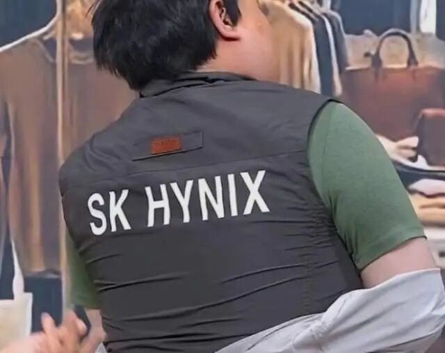
Source: Korean variety show
Kang Eun-sun, senior executive at Korean matchmaking firm Gayeon, publicly told media outlets that since the onset of the semiconductor supercycle, employees of Samsung Electronics and SK Hynix have seen a sustained surge in popularity. “The market clearly favors engineers whose actual incomes are significantly higher—more than lawyers whose earnings have declined relative to past levels.” Social media even spawned a meme: “When an SK Hynix employee goes on a blind date, they modestly claim to work at Samsung. Only when they find someone with good character do they honestly admit they’re actually at SK Hynix.”
What turned a standard uniform into a “blind-date battle armor” is a set of figures that make white-collar workers worldwide green with envy.
In 2025, SK Hynix’s operating profit reached ₩47.2 trillion (KRW). Per its new agreement with the labor union signed last September, 10% of operating profit flows into an employee bonus pool. With approximately 35,000 employees, each receives about ₩140 million—roughly RMB 650,000.
In Q1 2026, SK Hynix’s operating profit surged over 400% year-on-year to ₩37.6 trillion. Based on forecasts from analysts across various countries, its full-year 2026 operating profit is projected to land between ₩210 trillion and ₩250 trillion. By this estimate, per-employee bonuses for 2026 will range from RMB 2.9 million to RMB 3.3 million.
Macquarie Securities further predicts that operating profit will reach ₩447 trillion in 2027—potentially yielding per-employee bonuses as high as ₩1.29 billion, or approximately RMB 6.1 million.
Yet more compelling than the “RMB 6.1 million per-employee bonus” is this fact: this company had long been Korea’s number-two semiconductor player—the junior partner standing behind Samsung.
So what did it do right—causing even Samsung, whose screens and chips command Apple’s attention, to watch helplessly as it slipped from its position as the world’s memory霸主?
2008: Recovery from the Brink of Bankruptcy
Roll the clock back to 2008—and no one would have attached the label “future industry leader” to Hynix.
Its predecessor was Hyundai Electronics. During the 2001 dot-com bubble burst, DRAM prices plummeted, saddling the company with $14 billion in debt. Creditors took control, placing it under a five-year “workout program”—a Korean term akin to court-supervised restructuring. For five grueling years, its factories, R&D budgets, and staffing were all severely constrained.
By 2007, Hynix had finally emerged from this “restructuring” phase—but remained weak and barely surviving.
At precisely this moment, halfway across the Pacific, a company named AMD knocked on its door.
AMD’s situation wasn’t much better. As the #2 GPU vendor, it was being squeezed relentlessly by NVIDIA in the gaming graphics card market. Its researcher Bryan Black was developing something unconventional called “High Bandwidth Memory” (HBM)—stacking multiple DRAM dies vertically like floors in a building, interconnected via Through-Silicon Via (TSV) technology.
Why pursue this? Because AMD foresaw a problem most others overlooked: CPU/GPU compute speeds were accelerating rapidly, but memory data transfer rates couldn’t keep pace. Compute units frequently finished calculations only to idle while waiting for the next batch of data from memory—a bottleneck known in the industry as the “memory wall.”
To illustrate imperfectly: imagine a master chef slicing 10 dishes per second—but a delivery person bringing in only 2 ingredients per second. The chef ends up idle 80% of the time. No matter how fast the processor is, without timely data, it spins uselessly.
AMD’s solution was straightforward: rather than widening the horizontal transport channel (the traditional DDR approach), why not let memory “grow taller”—vertically stacking dies on-chip, shortening data travel distance and broadening the bus? This vertical “mini-skyscraper” is HBM.
The concept sounded elegant. But in 2008, there was zero AI demand, no large language model training, no so-called “compute revolution.” HBM’s only foreseeable application was high-end gaming GPUs—tiny market, extremely difficult manufacturing, and unit costs far exceeding conventional DRAM.
AMD pitched around—and no one bit. Samsung declined, fully committed to its alternative vertical-stacking technology, Hybrid Memory Cube (HMC), co-developed with Micron. Micron followed Samsung’s lead.
The sole willing partner was Hynix—freshly recovered from bankruptcy’s edge, desperate for any major order.
In 2009, Hynix officially launched its HBM R&D project. It wasn’t until 2013 that the first HBM chip rolled off Hynix’s production line in Icheon, South Korea.
Who could have imagined that this chip would, 15 years later, become a must-have commodity for every AI giant—so scarce that capacity is already sold out through 2030?
No one—not even Hynix itself.
2012: A Chairman’s High-Stakes Bet
In 2012, another pivotal figure entered the story.
Chey Tae-won, Chairman of SK Group, led a consortium anchored by SK Telecom to acquire a 21.05% stake in Hynix from creditors for roughly ₩3.4 trillion (about $3 billion). From then on, the semiconductor company became SK Hynix.
Who is Chey Tae-won? As described in the Korean book Super Momentum, shortly after the acquisition, he held one-on-one meetings with 100 Hynix executives within weeks. His first action wasn’t layoffs or cost-cutting—it was integrating SK Group’s management systems with Hynix’s technical capabilities, and restarting capital investment and process-improvement funding for fabs (fabrication plants).
The timing was critical.
From 2012 to 2014, the entire DRAM industry still languished in the shadow of the 2011–2012 memory downturn. Every rational financial model advised management: “This is the industry trough—play conservatively.” Yet Chey made the counterintuitive decision: expand investment.
Even more crucial was HBM.
Between 2011 and 2022—over 11 years—SK Hynix invested approximately ₩860 billion in HBM-related R&D and another ₩1.5 trillion in facilities and equipment. Much of this spending occurred during periods of market weakness, when HBM’s commercial viability seemed utterly remote.
What unfolded during those years?
HBM2 failed to meet performance targets and was scrapped and re-engineered into a revised version dubbed “HBM2 Gen2.” Within Hynix, the HBM team became “the department no one wanted to join.” Core staff were rotated out, morale sank. AMD’s flagship Radeon R9 Fury X GPU, launched in 2015, adopted first-generation HBM—but market reception was lukewarm due to its exorbitant price.
What unsettled Hynix even more occurred between 2016 and 2017: Broadcom approached Samsung, proposing that Samsung supply HBM2 for Google’s second-generation TPU. If Samsung could fulfill 100% of the demand, Broadcom promised exclusive supply rights—an opportunity that should have marked HBM’s breakthrough into data centers.
But Samsung dropped the ball.
A report by Korea’s JoongAng Daily reconstructed the ensuing chaos: Google’s TPU project involved three firms—Broadcom (design), Samsung (memory), and TSMC (foundry). Samsung’s HBM exhibited memory defects, and its engineers reported that TSMC refused them access to its facilities for onsite inspection. All three parties blamed each other, leaving the issue unresolved for up to six months. “Such gridlock was common between 2016 and 2017,” recalled a senior insider.
Google gradually shifted toward partnering with SK Hynix instead. HBM’s first genuine data-center deployment thus benefited Hynix—not Samsung.
Yet at the time, no one globally grasped that HBM would become the defining bottleneck of the AI era.
Chey later remarked in his Super Momentum interview: “We stood at a crossroads.”
He didn’t elaborate on why he persisted. In hindsight, the logic may have been this: Hynix’s fate had already teetered on bankruptcy’s edge once—in 2001. Unlike Samsung, it lacked diversified businesses to absorb risk. Memory was its sole domain. Either dominate it globally—or remain forever in Samsung’s shadow.
Thus, betting on HBM wasn’t a choice for Hynix. It had no alternative.
2022: Jensen Huang Hands Over a Matchstick
In June 2022, SK Hynix began mass-producing HBM3. That year, the first HBM3 chips were integrated into a GPU called the H100—manufactured by NVIDIA, a company then valued at roughly $300 billion, significant yet not world-altering in either gaming graphics or data centers.
In November, OpenAI launched ChatGPT.
What followed is well known: AI compute demand transformed from a gentle upward slope into a near-vertical rocket trajectory. Every GPU used to train large models requires HBM as its closest “data courier.”
At that moment, Hynix’s 14-year gamble suddenly paid off.
By Q2 2025, Hynix captured 62% of the global HBM market share. Samsung fell to 17%—even trailing newcomer Micron (21%).
For the full year 2025, Hynix’s operating profit totaled ₩47.2 trillion, versus Samsung Electronics’ ₩43.6 trillion. For the first time in history, Hynix surpassed Samsung in annual operating profit.
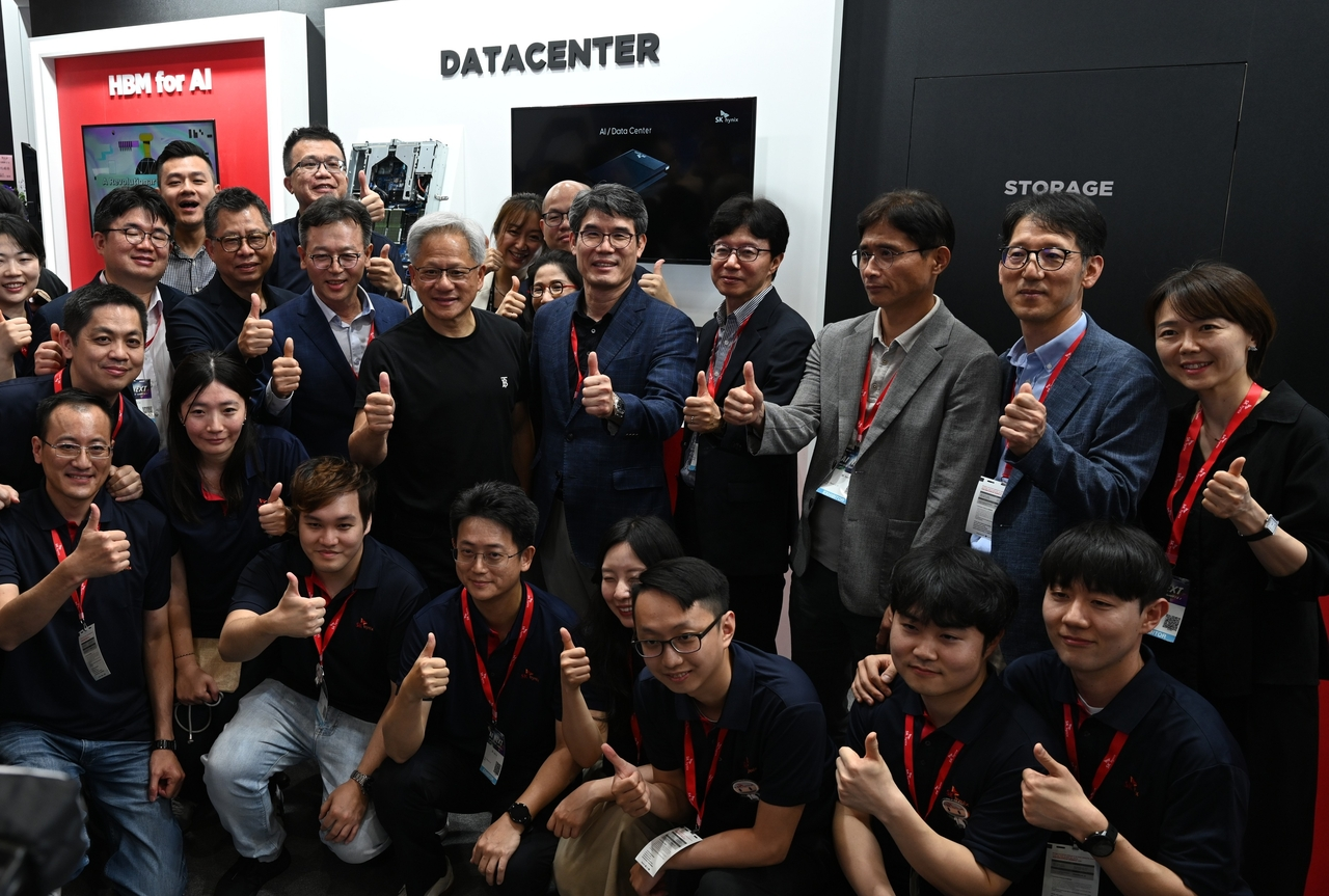
Jensen Huang, CEO of NVIDIA, visited SK Hynix’s booth at Computex Taipei in August 2025 and handwrote a message on its display board: "JHH LOVES SK HYNIX!" This photo quickly circulated across Korean media. In engineering culture, no endorsement is more direct or authoritative.
Hynix’s engineers, meanwhile, privately coined a new full form for HBM: “Hynix Best Memory.”
Where Did Samsung Go Wrong?
So the question arises: What went wrong for Samsung—the company that once crushed Japanese DRAM makers and cornered Micron?
Samsung missed early HBM positioning, chose the wrong packaging technology (NCF vs. Hynix’s MR-MUF), and repeatedly failed NVIDIA’s certification tests for HBM3E…
All true—but these aren’t root causes. The deeper, more ironic truth is this: Samsung was too successful—thus too risk-averse and unable to gamble.
Compare both companies in 2008. Hynix had just crawled out of bankruptcy proceedings, with memory as its only business line and no diversified cash cows to rely on.
Betting on HBM wasn’t about foresight—it was existential necessity. Any chance to shed the “junior partner behind Samsung” label had to be seized.
And Samsung?
In 2008, Samsung stood on the cusp of its golden age. Its mobile division was about to soar with the Galaxy series; its semiconductor business led globally in both DRAM and NAND; its display division was poised to secure Apple’s massive OLED orders for the iPhone. Its cash flow was abundant, its business portfolio vast, and its stakeholder interests incredibly complex.
For such a company, what was HBM in 2008? A high-risk, tiny-market, ultra-long-payback bet—one that directly conflicted with its flagship alternative technology (HMC). No rational finance committee would approve going “all-in” on it.
This is the classic “Innovator’s Dilemma”: successful large companies are perpetually constrained by their own success. Their existing markets are too large, too vital, too precious to protect—making it impossible for them to commit their entire future to a seemingly implausible new direction, as a “cornered challenger” might.
The deeper irony? Samsung didn’t ignore HBM. It began investing in related R&D as early as 2011 and even pioneered HBM2 mass production in 2016. But each time, it stopped short of “all-in.” Its focus remained fragmented across HMC, GDDR, LPDDR, enterprise SSDs, and over a dozen other fronts. While Hynix’s HBM team was “marginalized yet persisting,” Samsung’s HBM team was also “marginalized”—but no one was left to push forward.
By 2024–2025, Samsung finally realized it must go “all-in” on HBM—but it was too late. The technological gap had solidified; the customer-relationship moat had already been jointly built by NVIDIA and Hynix.
Jun Young-hyun, Vice Chairman of Samsung Electronics’ Semiconductor Division, stated in his 2026 New Year address: “Customers tell us, ‘Samsung is back.’”
That single word—“back”—is itself an admission.
Two Questions
What does SK Hynix’s story signify? At least two questions merit attention.
First, why do similar stories occur more readily in Korea than elsewhere?
Hynix’s success didn’t happen in a vacuum. It grew in a unique industrial ecosystem. Though Korea’s chaebol system has drawn criticism for decades, objectively it allows a single decision-maker to commit to a 20-year bet—and sustain funding through ten years of zero commercial visibility.
When Chey acquired Hynix in 2012, no Wall Street analyst shouted “quarterly earnings! quarterly earnings!” He bore no obligation to justify HBM’s ROI to his board every quarter.
Such long-term decision-making cycles are increasingly rare among today’s U.S.-market-driven tech firms. They’re also a key variable determining whether China’s hard-tech players—like Yangtze Memory Technologies (YMTC) and CXMT—can break through. Technology isn’t the biggest barrier; the willingness of capital and leadership to sit through a decade of obscurity is.
Second, has Hynix truly escaped its “number-two” fate?
Not necessarily.
By Q4 2025, Samsung had reclaimed the top spot globally in total memory revenue. It’s accelerating its HBM4 development, with key certifications nearing approval. MS Hwang, Research Director at Counterpoint, assesses that Samsung may overcome last year’s quality issues in the HBM4 generation and achieve a meaningful turnaround.
Longer term, Hynix’s current moat has vulnerabilities: extreme customer concentration (NVIDIA accounts for a huge portion of orders), warping challenges with its MR-MUF packaging beyond 16-layer stacks, and rising expansion costs that will pressure free cash flow in 2026–2027. Chinese competitors are advancing too—CXMT expects to begin HBM mass production in 2027. Once that line breaks through, the global HBM oligopoly will shift again.
Yet none of this changes one fundamental fact: SK Hynix has proven a possibility—that a perennial “number-two,” long dismissed as forever trailing a giant, can, over two decades of ridicule, transform itself into the architect of a new era.
A market principle is reaffirmed: when everyone chases certainty, betting on a seemingly uncertain long-term direction often yields the greatest alpha.
This was HBM in 2008. It was the new-energy-vehicle supply chain in 2018. In 2026, it may be something else entirely—still unappreciated by anyone today.
Don’t ask, “Who is today’s SK Hynix?” Instead, ask: Who today is doing exactly what SK Hynix did in 2008—yet being laughed at by everyone?
Join TechFlow official community to stay tuned
Telegram:https://t.me/TechFlowDaily
X (Twitter):https://x.com/TechFlowPost
X (Twitter) EN:https://x.com/BlockFlow_News